STE Highlights, February 2023
Awards and Recognition
Earth and Environmental Sciences
Study provides new method for generating high-resolution snow cover maps
Materials Physics and Applications
Inducing ferromagnetism in epitaxial uranium dioxide thin-film actinides
Metal cathode surfaces protected with Atomic Armor maintain emittance performance
Asymmetry of magnetic proximity interaction offers routes for control in semiconductors
Photocathodes encapsulated with graphene and thin metal film meet technical challenges
Awards and Recognition
Wohlberg named an IEEE Fellow

Brendt Wohlberg
Brendt Wohlberg, a staff scientist in the Applied Mathematics and Plasma Physics group (T-5) in Theoretical Division, has been named a Fellow of the IEEE. The IEEE Fellowship is awarded to members “with an extraordinary record of accomplishments in any of the IEEE fields of interest.” A select group, each year less than one-tenth of one percent of the IEEE voting membership may be selected for elevation to Fellow.
Wohlberg was selected as an IEEE Fellow “for contributions to computational imaging and sparse representations.” One of his most significant contributions to computational imaging was as one of the developers of the plug-and-play priors method, a flexible algorithmic framework that allows state-of-the-art forward models of imaging systems to be matched with state-of-the-art priors or denoising models. The technique is widely used for imaging inverse problems, with real-world applications including use in the ultrasonic fingerprint sensing component of a recent cellular phone chipset.
His significant contributions to sparse representations include the development of new algorithms and methods the convolutional form of sparse representations and dictionary learning. An open-source implementation of these algorithms has found wide adoption, with more than 200,000 downloads to date. Much of the research in both of these areas has been supported by the Laboratory Directed Research and Development program.
Wohlberg is a graduate of the University of Cape Town, South Africa, earning a doctoral degree in electrical engineering. After a postdoctoral research fellowship at the University of Cape Town, he worked as a postdoctoral research associate in the Laboratory’s Center for Nonlinear Studies from 1999 to 2002. He joined Theoretical Division as a scientist in 2002.
Wohlberg was a corecipient of the 2020 SIAM (Society for Industrial and Applied Mathematics) Activity Group on Imaging Science Best Paper Prize. He was an associate editor for IEEE Transactions on Image Processing from 2010 to 2014, and for IEEE Transactions on Computational Imaging from 2015 to 2017. He chaired the Computational Imaging Special Interest Group of the IEEE Signal Processing Society from 2015 to 2017. He was editor-in-chief of IEEE Transactions on Computational Imaging from 2018 to 2021, and is currently editor-in-chief of IEEE Open Journal of Signal Processing.
Chen named Nanomaterials 2022 Young Investigator Award winner

Aiping Chen
Los Alamos National Laboratory scientist Aiping Chen, with the Center for Integrated Nanotechnologies, has been named a recipient of the Nanomaterials 2022 Young Investigator Award. Chen joins two other researchers in receiving the honor from Nanomaterials, an international, peer-reviewed journal publishing on the synthesis and use of nanomaterials.
At the Center for Integrated Nanotechnologies, Chen leads efforts on the synthesis and characterization of complex oxide heterostructures and nanocomposites. The author of more than 120 published papers cited more than 4,600 times, Chen’s recent research focuses on thin film synthesis, emergent phenomena in quantum materials and electronic devices. Nanomaterials noted, “His work has impacted the epitaxial growth of complex metal oxide thin films and nanostructured materials using pulsed laser deposition and laser molecular beam epitaxy.”
Chen received his doctoral degree in electrical engineering from Texas A&M University in 2013 before joining the Laboratory as a postdoctoral research associate. He received a Director’s Postdoctoral Fellowship in 2014 and was converted to a scientist in the Center for Integrated Nanotechnologies in 2016.
Bioscience
Research uses deep neural network to identify replacement bioplastics
The combination of 540 polyhydroxyalkanoate (PHA) biopolymers and 13 conventional, fossil-derived polymers to copolymers creates a large search space. Bioplastic candidates within the search space are identified with property predictors and property requirements of commonly used polymers.
Plastics help sustain many facets of modern lifestyles and current technologies, at the cost of generating environmentally harmful plastic waste. To identify bio-synthesized and biodegradable alternatives to plastics from among natural, microorganism-produced polymers called polyhydroxyalkanoates (PHAs), Los Alamos National Laboratory researchers have developed multitask deep neural network property predictors. In research described in Communications Materials, the team used those predictors to identify 14 PHA-based bioplastics that could replace nearly 75 percent of the world’s plastic production.
Global plastic production as recently as 2019 totaled 368 million tonnes. Packaging products — bottles, bags, cutlery, food containers and other products — account for approximately 40 percent of that total. With short service lifetimes, such products and their attendant microplastic particles threaten the world’s ecosystems. PHAs, synthesized for example, by photosynthetic microorganisms naturally using sunlight and carbon dioxide as a carbon source offer plastic replacement potential with sustainable recycling options. Experimentation on PHAs is constrained by their chemical complexity and diversity, so the research team developed multitask deep neural network property predictors. Those predictors were able to tackle nearly 23,000 homo- and copolymer chemistry data points spanning 13 critical properties.
The 23,000 experimental data points were used to develop efficient multitask deep neural network-based multiproperty predictors for copolymers that forecast three different thermal, four different mechanical, and six gas permeability properties. The team’s state-of-the-art polymer informatics approach used multitask neural networks with a meta learner to forecast properties from among nearly 1.4 million polymers in a bioplastic candidate space. The properties and their combinations present critical design parameters for plastics. The study then followed a two-step protocol of a nearest neighbors search and synthesizability criteria to find several PHA-only and PHA-conventional polymer bio-replacements in the candidate space for seven petroleum-based and commonly used plastics — the seven petroleum-based plastics accounting for 75 percent of the world’s plastic production. The informatics approach also informs possible synthesis routes for the bio-replacements.
The work may augment other design approaches and accelerate the identification and development of bioplastics that offer improved functionality and sustainable recycling as part of the transition to a circular economy.
Funding and mission
This work is supported by the Laboratory Directed Research and Development program at Los Alamos, the Alexander von Humboldt Foundation and the Office of Naval Research in the U.S. Department of the Navy. This work supports the Global Security mission area and the Complex Natural and Engineered Systems capability pillar.
Reference
“Bioplastic design using multitask deep neural networks,” Communications Materials, 3, 96 (2022); DOI: 10.1038/s43246-022-00319-2. Authors: Christopher Kuenneth, Jessica Lalonde, Babetta L. Marrone, Carl N. Iverson and Ghanshyam Pilania (Los Alamos National Laboratory); and Rampi Ramprasad (Georgia Institute of Technology).
Technical Contact: Babetta Marrone (B-IOME)
Earth and Environmental Sciences
Study provides new method for generating high-resolution snow cover maps

Example of snow cover detection using the newly developed method for a GeoEye image taken of a location near Cook Inlet, Alaska. The true-color image on the left shows the extent of snow (white areas) and the image on the right shows the predicted snow-covered areas (blue).
Remote sensing tools provide a powerful method for mapping snow-covered area across a landscape. The most common method for estimating snow-covered area utilizes the normalized difference snow index, which relies on spectral measurements in the shortwave-infrared wavelengths. Application of the normalized difference snow index is limited to regional and watershed-scale assessments of snow-covered area because of current limitations on the spatial resolution of satellite-derived shortwave infrared measurements. To overcome this limitation, scientists from the Climate, Ecosystems, and Environmental Science group (EES-14) in the Earth and Environmental Sciences Division at Los Alamos National Laboratory have developed a new method, an algorithm dubbed the Blue Snow Threshold, for using satellite imagery to map snow-covered area at resolutions 10 times greater than previous methods.
As described in a new publication in the journal Remote Sensing of Environment, the Blue Snow Threshold algorithm uses only the blue wavelengths from cloud-free high-resolution satellite imagery to partition an image into snow and non-snow pixels. The new algorithm predicts snow-covered area with an approximately 90 percent accuracy when compared to lidar surveys of snow cover, which are considered the industry standard ground-truth data. Because of the availability of high-resolution satellite imagery, the new method can be applied to assess fine-scale changes in snow cover and examine the impacts of climate-driven changes on hydrology, ecosystem processes and the stability of permafrost soils.
Snowfall is a critical component of the hydrologic cycle, the global climate system and ecosystem function. For example, snow is the dominant source of groundwater recharge and streamflow in mountainous landscapes. Snow is also an efficient insulator and can keep soils warm in the winter, causing thawing of permafrost soils and potentially emitting greenhouse gases. The magnitude of snowfall, duration of snow cover and timing of snowmelt are all expected to shift dramatically under climate change. Therefore, developing high-resolution assessments of snow cover change is crucial for estimating the impact of changing snow cover on the hydrologic system, as well as for understanding other fundamental processes, such as the impact of snow cover on the thermal stability of permafrost soils.
Funding and mission
This research was supported by the U.S. Department of Energy's Office of Science Office of Biological and Environmental Research as a contribution to the Next Generation Ecosystem Experiment-Arctic project. The work supports the Global Security mission area and the Complex Natural and Engineered Systems capability pillar.
Reference
“Estimating snow cover from high-resolution satellite imagery by thresholding blue wavelengths,” Remote Sensing of Environment 285 (2023); DOI: 10.1016/j.rse.2022.113403. Authors: Evan A. Thaler, Ryan L. Crumley, and Katrina E. Bennett (Los Alamos National Laboratory).
Technical contact: Evan Thaler (EES-14)
Materials Physics and Applications
Inducing ferromagnetism in epitaxial uranium dioxide thin-film actinides
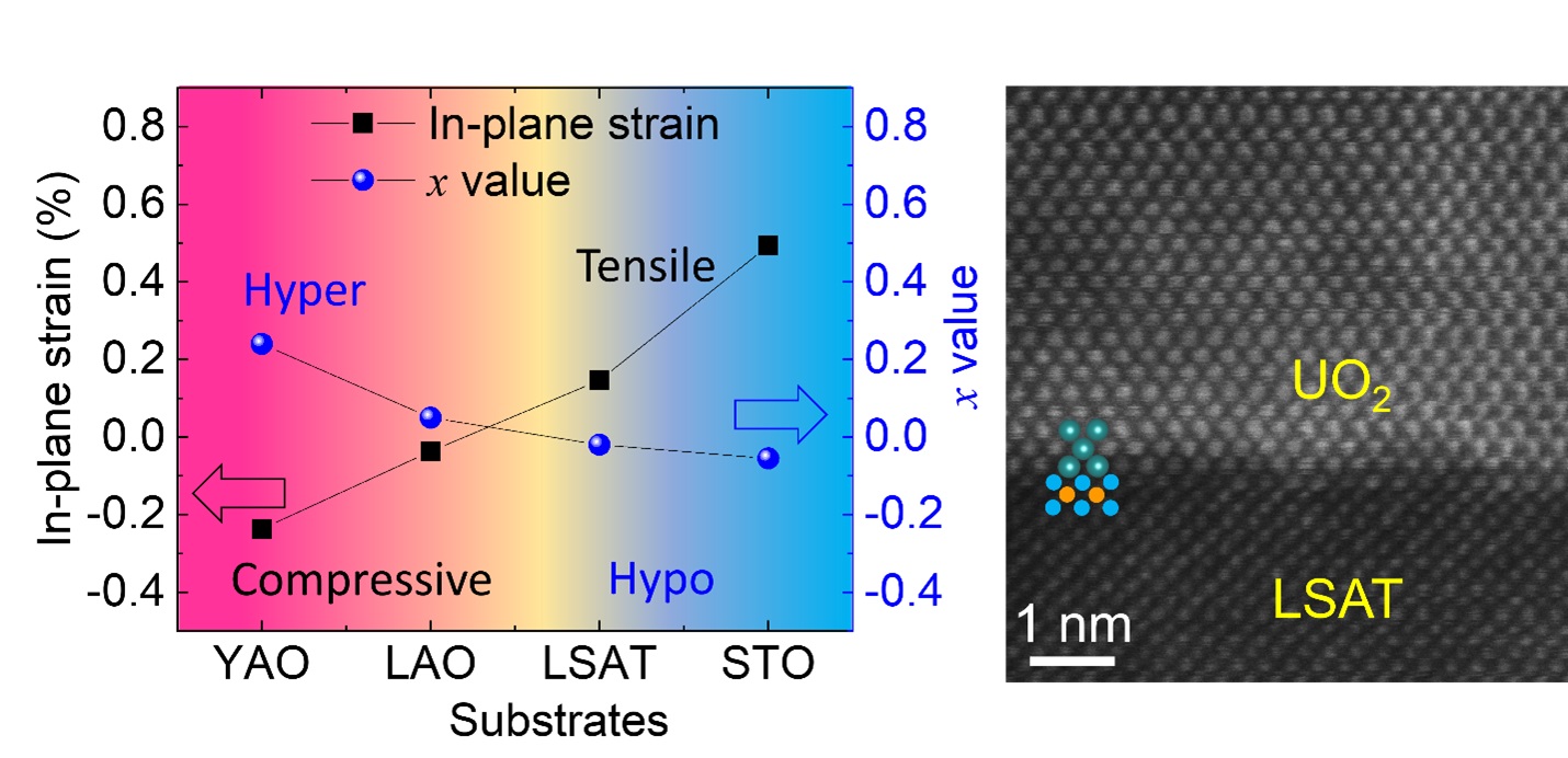
Left: strain tuning of oxygen stoichiometry in uranium dioxide; Right: a high-resolution scanning transmission electron microscopy image of UO2 films.
Motivated by the breakthroughs over the past decades in complex oxides enabled by thin-film growth technology, a team of Los Alamos materials researchers and external colleagues used the Laboratory’s actinide thin-film capability to explore strain engineering on epitaxial actinide thin films. Strain engineering has been widely used to tune functional properties or create exotic phenomena in thin films, but its application to actinide materials has been sparse.
Published in Advanced Science, the work reveals the correlation among strain, point defects and ferromagnetism in strain engineered uranium dioxide. The team investigated the origin of induced ferromagnetism, or permanent magnetization, in an antiferromagnet uranium dioxide. (Antiferromagnetism is an alignment of electrons resulting in a magnetic moment of zero.) The oxide was chosen due its fundamental interest as a strongly correlated material — a type of material with unusual electronic and magnetic properties — with theoretical studies proposing unique functionalities. The results offer new opportunities to understand the influence of coupled order parameters on the emergent properties of many other actinide thin films.
Actinide materials are an important part of modern technology, playing crucial roles in applications ranging from nuclear energy to quantum computing. Despite this range of service, state-of-the-art research efforts are mainly limited to bulk actinide materials. Extensive theoretical efforts exploring thin-film actinide properties have been made in the past decades, but the research described in Advanced Science represents one of the few experimental studies on physical behaviors that emerge through strongly coupled structural, electronic and magnetic degrees of freedom.
The research team used the Lab’s high-resolution scanning transmission electron microscopy to characterize the film microstructure and the quality of the film-substrate interface of the uranium dioxide films. This work also leverages advanced thin-film synthesis and characterization capabilities at the Center for Integrated Nanotechnologies including pulsed laser deposition, high-resolution thin film x-ray diffractometer and physical property measurement system.
Funding and mission
The Los Alamos portion of the work was funded by the Laboratory Directed Research and Development Program and was performed, in part, at the Center for Integrated Nanotechnologies, a DOE Office of Science user facility operated jointly by Sandia National Laboratories and Los Alamos National Laboratory. This work is also partially funded by the Seaborg Institute, the U.S. Department of Energy and the National Science Foundation. The work supports the Laboratory’s Energy Security mission and the Materials for the Future capability pillar.
Reference
“Induced ferromagnetism in epitaxial uranium dioxide thin films,” Advanced Science, 9, 33 (2022); DOI: 10.1002/advs.202203473. Authors: Yogesh Sharma, Binod Paudel, Matthew M. Schneider, Rico Schönemann, Andrew C. Jones, Marcelo Jaime, Dmitry A. Yarotski, Michael T. Pettes, Ping Yang and Aiping Chen (Los Alamos National Laboratory); Amanda Huon and Timothy Charlton (Oak Ridge National Laboratory); Pinku Roy, Zachary Corey and Quanxi Jia (University at Buffalo); and Michael R. Fitzsimmons (University of Tennessee).
Technical contact: Aiping Chen (MPA-CINT)
Metal cathode surfaces protected with Atomic Armor maintain emittance performance
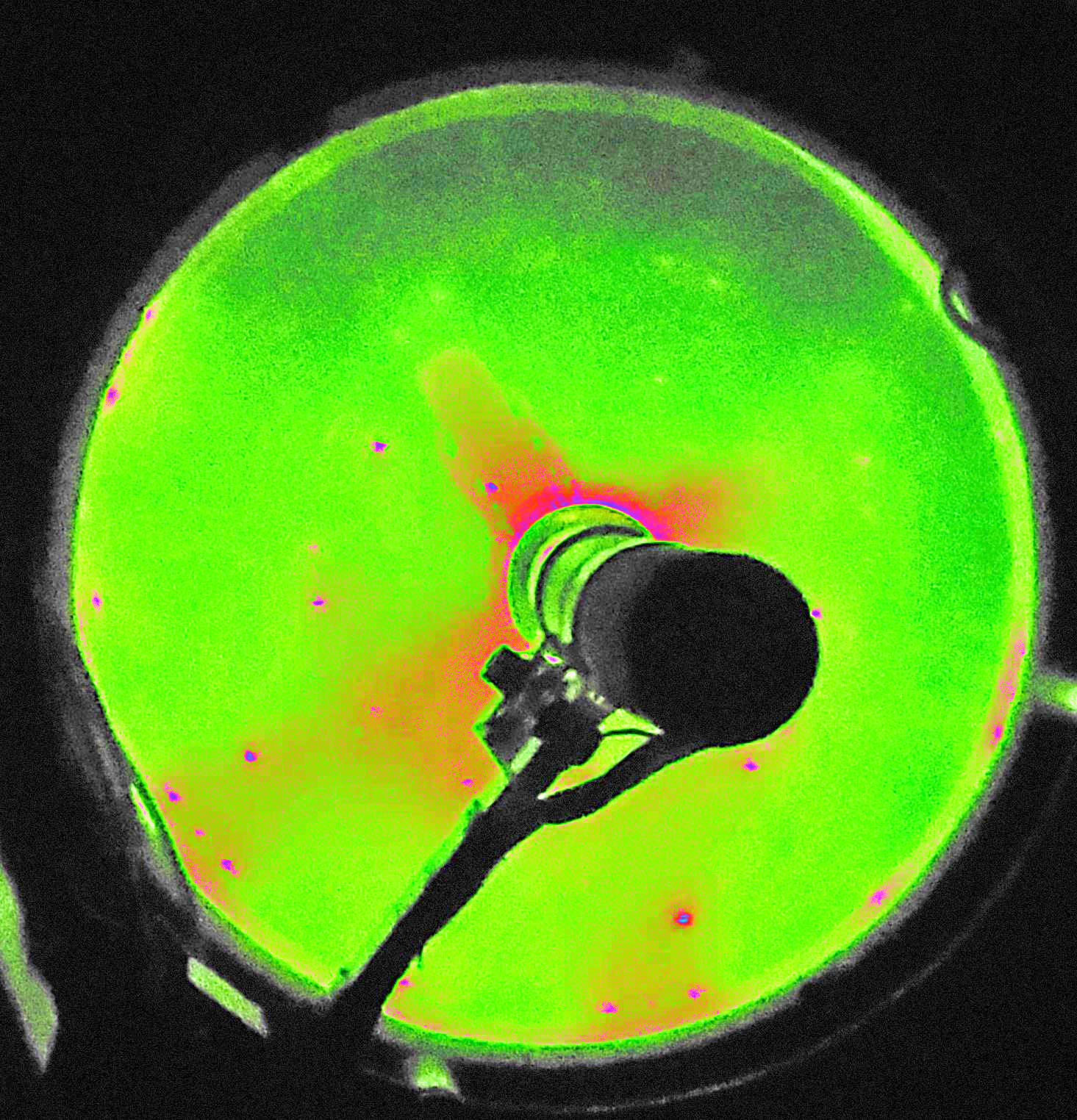
The low-energy electron diffraction (LEED) pattern collected at 155 electron volts. Higher-order diffraction is shown, a pattern in agreement with previously measured LEED patterns from graphene-coated Cu(110).
The brightness of pulsed electron beams generated from photoinjectors is a critical factor in experiments with x-ray free-electron lasers and ultrafast-electron-diffraction and ultrafast-electron-microscopy.
With the cleanest possible materials surfaces, an accelerator’s lowest emittance — the narrowness of the energy spread, or mean transverse energy (MTE) — helps achieve maximum electron beam brightness.
New research from a team including Los Alamos scientists has investigated the effect of a coating of Atomic Armor, an atomically thin layer of graphene, on an accelerator’s mean transverse energy. To create the cleanest possible surfaces and achieve the required brightness, accelerator operators have been treating a surface of single crystal metal with time- and effort-consuming multiple cycles of argon sputtering/ion bombardments and annealing at a high temperature (600 degrees Celsius). Alternatively, as described in Physical Review Applied, the research team found that the lowest mean transverse energy can be achieved by simply coating a single crystal metal surface with atomically thin graphene and a one-time heating at a lower temperature, 345 degrees Celsius.
The research measured a graphene-coated Cu(110) single crystal near the photoemission threshold for room and liquid-nitrogen temperatures At room temperature, a minimum MTE of 25 millielectron volts was measured at 295 nanometers. At liquid-nitrogen temperatures, a minimum MTE of 9 millielectron volts was measured at the photoemission threshold of 290 nanometers. (The photoemission threshold is the energy sufficient to eject an electron from a solid or liquid in photoemission.) The results signify the first-ever protection of metal cathode surfaces using atomically thin material, graphene, while maintaining the performance of mean transverse energy, emittance.
The thermal limit of 25 millielectron volts at room temperature being consistently measured for seven days indicated the extreme stability of the cathode. The coating protected the surface to maintain its cleanness even when exposed to air. The graphene coating also simplifies the surface preparation required to achieve a well-ordered single-crystal. That convenience contributes to the viability of graphene-coated single crystals as an option for current and future photoinjectors.
Reference
“Near-Threshold Photoemission from Graphene-Coated Cu(110),” Physical Review Applied, 19, 014015 (2023); DOI: 10.1103/PhysRevApplied.19.014015. Authors: Christopher J. Knill and Siddharth Karkare (Arizona State University); Hisato Yamaguchi, Gaoxue Wang, Enrique Batista, Ping Yang, Nathan Moody (Los Alamos National Laboratory); and Kenji Kawahara and Hiroki Ago (Kyushu University).
Funding and mission
This work was supported by the U.S. National Science Foundation, by the Center for Bright Beams, Department of Energy Office of Basic Energy Sciences, the U.S. Department of Energy (DOE) Office of Science under the U.S.-Japan Science and Technology Cooperation Program in High Energy Physics, the Japan Society for the Promotion of Science, the Laboratory Directed Research and Development Program, and the G. T. Seaborg Institute at the Laboratory.
Technical Contact: Hisato Yamaguchi (AOT-AE)
Asymmetry of magnetic proximity interaction offers routes for control in semiconductors
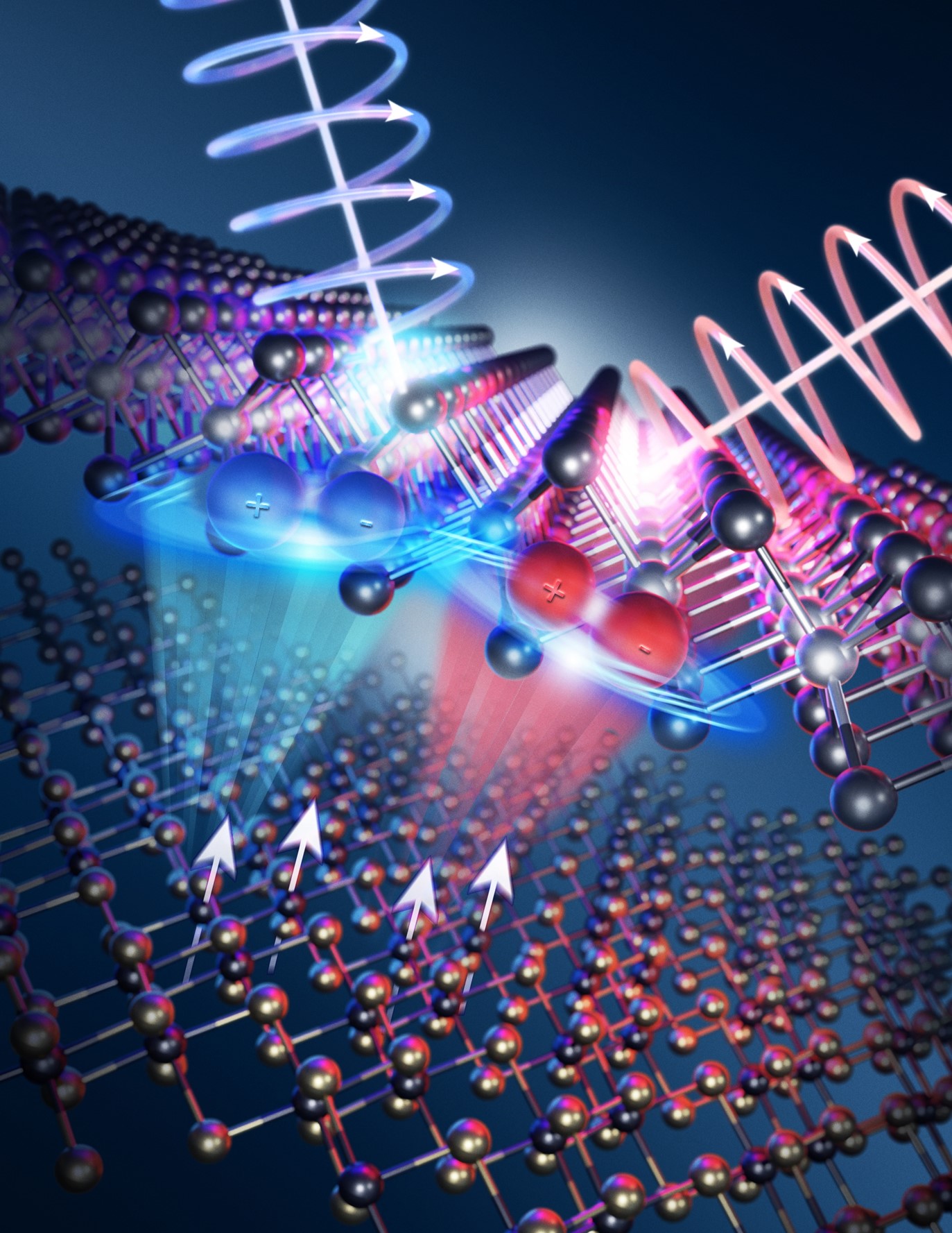
Single 2D monolayers of the semiconductor MoSe2 were stacked atop thin ferromagnetic CrBr3 via van der Waals assembly. Optical spectroscopy using right-circular and left-circularly polarized light revealed and quantified MPIs for both spin-up and spin-down excitons in the MoSe2 monolayer (red and blue, respectively). [Image: Sarah Tasseff, Los Alamos National Laboratory]
The ability to impart magnetic functionality into otherwise non-magnetic materials has exciting prospects for hybrid devices that combine, for example, the optical and electrical properties of semiconductors with additional tuning parameters that couple to magnetic and spin degrees of freedom. New research published in Nature Materials by a Los Alamos team explores these interesting “magnetic proximity interactions” (MPIs) in layered stacks comprising magnetic and non-magnetic 2D materials, suggesting routes to control electron spins in nominally non-magnetic semiconductors, without the use of applied magnetic fields.
As recent work has demonstrated, MPIs can be achieved by placing an atomically thin sheet of semiconductor crystal directly atop the clean crystalline surface of a ferromagnet. The intimate proximity of the two materials allows for the electrons in the two materials to “see” each other and interact quantum mechanically. The hybrid structure is held together only by weak van der Waals interactions between the two layers, rather than actual chemical bonds. These so-called “van der Waals heterostructures” are assembled layer-by-layer by mechanical stacking of individual 2D crystals of the constituent materials. In sufficiently clean structures having pristine interfaces, MPIs originate in the nanometer-scale coupling between the spin-dependent electronic wavefunctions of the two materials. Historically, the influence of such MPIs has been regarded as an effective magnetic field acting on the nominally nonmagnetic semiconductor.
But the Los Alamos team’s work showed that the widely held picture of effective magnetic fields, while useful, is in fact fundamentally incomplete. Rather, the influence of MPIs is actually quite asymmetric. That is, electrons with spin-up and spin-down are not affected equally and oppositely, as would be the case for a real magnetic field. The team used circularly polarized optical spectroscopy of MoSe2/CrBr3 van der Waals structures to reveal strikingly different energy shifts for spin-up and spin-down excitons (electron-hole pairs) in the MoSe2 semiconductor layer, due to MPIs from the ferromagnetic CrBr3 layer. Importantly, spin-asymmetric MPIs were confirmed by density functional theory calculations, and shown to depend sensitively on the spin-dependent hybridization of overlapping electronic bands in the two materials. As such, asymmetric MPIs are likely a general feature of all magnetic/nonmagnetic hybrid van der Waals structures.
An important implication of the research is the possibility to selectively control specific spin states (and associated valley degrees of freedom) in 2D semiconductors through rational design of component materials and their stacking arrangement. Such combinations open up new possibilities for combining functionality such as information processing and nonvolatile storage.
See also News and Views feature, "Asymmetry in the Magnetic Neighborhood," in Nature Materials, authors T. Zhou & I. Zutic (University at Buffalo).
Reference
“Asymmetric magnetic proximity interactions in MoSe2/CrBr3 van der Waals heterostructures,” Nature Materials (2022); DOI: 10.1038/s41563-022-01424-w. Authors: Junho Choi, Christopher Lane, Jian-Xin Zhu and Scott A. Crooker (Los Alamos National Laboratory).
See also News and Views feature, "Asymmetry in the Magnetic Neighborhood," Nature Materials (2023); DOI: 10.1038/s41563-022-01466-0. Authors: T. Zhou and I. Zutic (University at Buffalo).
Funding and mission
Experimental studies at the National High Magnetic Field Laboratory were supported by the Los Alamos Laboratory Directed Research and Development program. The National High Magnetic Field Laboratory is supported by National Science Foundation (DMR-1644779), the state of Florida and the U.S. Department of Energy. Computational studies were supported in part by the Center for Integrated Nanotechnologies, a U.S. Department of Energy Basic Energy Sciences user facility, in partnership with the Los Alamos National Laboratory Institutional Computing Program for computational resources. Additional computations were performed at the National Energy Research Scientific Computing Center, a U.S. Department of Energy Office of Science user facility using National Energy Research Scientific Computing Center support. This work supports the Global Security mission area and the Materials for the Future capability pillar.
Technical contact: Scott Crooker (MPA-MAGLAB)
Photocathodes encapsulated with graphene and thin metal film meet technical challenges
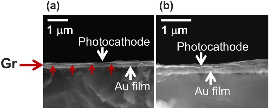
The image in (a) shows the photocathodes deposited on a graphene substrate, while (b) shows a non-coated gold substrate. The red arrows in (a) indicate the graphene coating. Scale bars are one micrometer. Image used under Creative Commons license.
The performance and longevity of free-electron sources, including accelerators in demand for a broad range of research and development applications, presents a technical challenge. A team led by Los Alamos researchers has been developing two-dimensional materials that mitigate photocathode corrosion and degradation from gas molecules while allowing for high quantum efficiency electron transmission. By sandwiching high quantum efficiency bialkali photocathodes in between graphene and thin nickel film as the protective encapsulation, the team demonstrated a three orders of magnitude improvement in active pressure and a lifetime enhancement for the photocathodes of a factor of two.
First discovered in the 1950s, bialkali antimonide high quantum efficiency semiconductor photocathodes have long been used as photosensitive materials in radiation detectors and camera tube technologies. Recently they have been explored for use in advanced accelerators and electron microscopes, which require high-brightness electron bunches in short pulses. The use of cesium potassium antimonide as an electron source for next-generation accelerators holds promise due to the material’s balance between quantum efficiency and operation pressure. The low operation pressure of 10–8 Pa and the short operation lifetime of the photocathodes do still present a technical challenge, though. Replacing photocathodes incurs a cost of time and expense, so protecting free electron sources means longer lifetimes for the photocathodes and a potential broadening of the accelerators in which they can be used.
Two-dimensional materials such as graphene uniquely possess the critical material properties of electron/photon transmissivity and gas impermeability. Graphene’s packed hexagonal atomic structure makes it impermeable to gases, and its atomic thinness makes it photon and electron transparent. To evaluate graphene’s feasibility for use as a protective layer for bialkali antimonides, the team deposited photocathodes on a free-standing bilayer of graphene and sealed them with a 15–35 nm thick nickel films. As described in a recent issue of Scientific Reports, the team observed significant improvements in active pressure and in lifetime enhancement. The results are seen as promising for meeting the approximately two-week turnaround time for feasible operation of accelerators using high-brightness bialkali photocathodes.
Funding and mission
The work was supported by the U.S. Department of Energy Office of Science under the U.S.-Japan Science and Technology Cooperation Program in High Energy Physics, the Laboratory Directed Research and Development Program at Los Alamos National Laboratory, and the High Energy Accelerator Research Organization in Japan. This work was performed, in part, at the Center for Integrated Nanotechnologies, an Office of Science User Facility operated for the DOE Office of Science by Los Alamos National Laboratory. The work supports the Global Security mission area and the Materials for the Future capability pillar.
Reference
“Rugged bialkali photocathodes encapsulated with graphene and thin metal film,” Scientific Reports, 13, 2412 (2023); DOI: 10.1038/s41598-023-29374-6. Authors: Lei Guo and Yoshifumi Takashima (Nagoya University Synchrotron Radiation Research Center); Fangze Liu (Beijing Institute of Technology); Kazuki Koyama (Nagoya University); Nolan Regis, Anna M. Alexander, Gaoxue Wang, James A. Valdez, Anju Poudel, Nathan A. Moody and Hisato Yamaguchi (Los Alamos National Laboratory); Jeffrey DeFazio (Photonis Defense, Inc.); and Masahiro Yamamoto (High Energy Accelerator Research Organization).
Technical Contact: Hisato Yamaguchi (AOT-AE)


